PCB Design Guidelines for EMIEMC Circuit Diagram Dealing with EMI in PCB design is a crucial aspect of creating reliable, high-performance embedded systems. By understanding the sources of EMI and implementing best practices like optimized stack-up, proper grounding, trace layout, and shielding, engineers can design noise-free PCBs that meet performance and compliance requirements.

Mastering high-speed PCB routing techniques for EMI reduction is crucial in today's electronic design landscape. By implementing the strategies outlined in this guide - from optimizing layer stack-ups and differential pair routing to careful power distribution and post-layout mitigation techniques - designers can significantly reduce the
PCB Design Guidelines for EMI Reduction and EMC Optimization Circuit Diagram
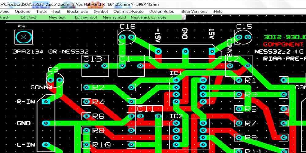
PCB Layout Techniques for Minimizing Crosstalk and EMI . Fortunately, a well-crafted PCB layout strategy can significantly reduce crosstalk and EMI. Here are some key techniques to consider: 1. The Power of the Ground Plane . The ground plane is an often overlooked yet essential element in PCB design. 7 design guidelines for EMI and EMC reduction in a PCB. How do you design a board with low or absolutely zero electromagnetic interference? Well, it isn't impossible. The design practices below will make sure you do not create antennas that emit electromagnetic energy. These best design practices will reduce the length and area of the
High-frequency signals or large current spikes can produce strong electromagnetic fields that may interfere with nearby electronic components, leading to EMI. PCB Stack-up and Layer Configuration. A well-planned PCB stack-up can significantly reduce EMI. A typical multilayer PCB consists of signal layers, power planes, and ground planes.
PCB Layout Techniques for Minimizing Crosstalk and Electromagnetic ... Circuit Diagram
Discover PCB design practices for reducing EMI and improving EMC. Optimize your designs with component isolation, EMI filtering, and OrCAD X tools. Learn essential PCB design guidelines for EMI reduction, enhance EMC, and achieve reliable signal integrity. Explore strategies for components, layout, and OrCAD X. It is best to use separate Shielding can be very effective, but it is never a good idea to rely on a shield to solve all EMI issues. This is very often not a viable solution and the best idea is always to use best practices for PCB design and layout, and use shielding as a backup or an additional layer of protection. 9. Impedance Control EMC Issues In PCB Design. EMC problems in PCB design can arise from a number of causes, including: 1. High-speed signals: These signals have the potential to emit electromagnetic energy/ noise that might obstruct the operation of other PCB components or external devices. 2.